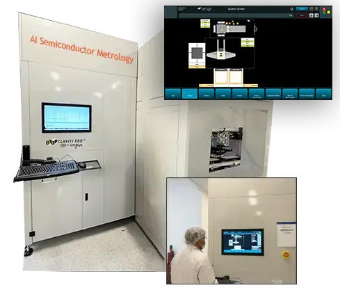
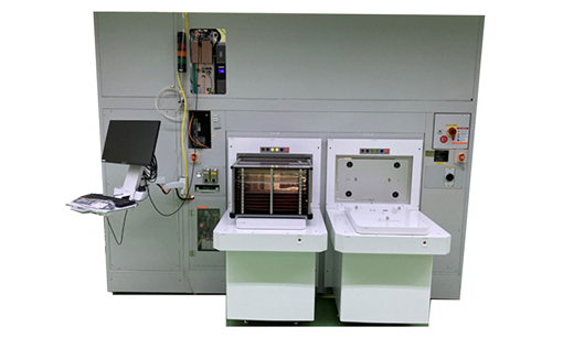
Next-Generation Glass Defect Inspection using AI
Glass Defect Inspection with sub-micron capability
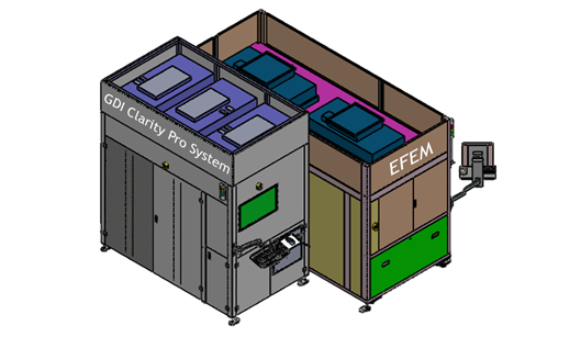
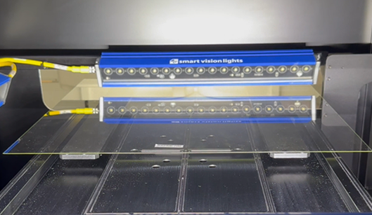
GDI Clarity Pro redefines precision in glass defect inspection with cutting-edge optics and advanced surface scanning. Capable of detecting defects as small as sub-micron levels with a spatial resolution of 2.5 µm, it delivers unmatched edge and through-surface defect analysis. Defect classification & measurement done real-time, with no throughput overhead.
The system offers:
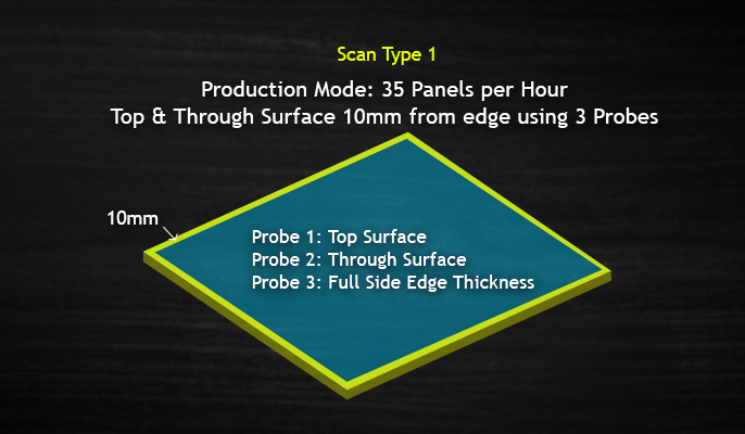
- Production Mode: 35 Panels per Hour, Edge inspection Top & Through Surface 10mm using 3 Probes
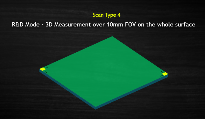
- Advanced R&D mode with 2D and 3D inspection capabilities with Z-axis resolution of <1 nanometer
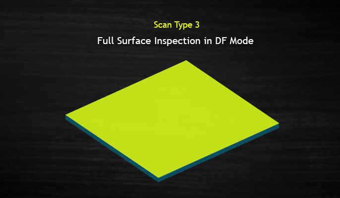
- Full-panel macro-surface scanning for holistic defect identification
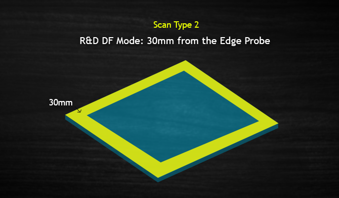
- 30mm edge-detection range for surface inspection
Engineered for Semiconductor industries demanding the highest quality. GDI Clarity Pro brings absolute transparency to defect detection.
How it works
Highlights
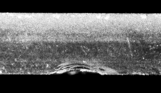
DEFECTS ON GLASS SUBSTRATES
Chips <1 μm
Edge defects <1 μm
Cracks <1 μm length and ≥5 μm depth (in Z)
Scratches <1 μm length and <5 μm depth (in Z)
FM (foreign material) <1 μm
Surface Pitting <1 μm
Stains and FM are classified separate from other defect types
Classification >5 μm
E-MCBFp* > 20,000 cycles with uptime >95%
Supplier dependent scheduled downtime <1%
Substrate Form Factor Size(s) Less than 520mm
Production Run Rate 35 full substrates/hour
Automatic Defect Classification (ADC) Yes
Image Processing Fully Trained AI
Defect Size Repeatability 3-sigma < 10%
Same defect measured at least 20 times to calculate 3-sigma.
Defect Image Capture
Variable magnification review image automatically
saved for visual defect review/classification
R&D Applications
3D-Profile(Mapping) with Z-Height Measurement (>1nm)
Active Area Surface 10mm Inspection Sampling
Equipment Matching/Calibration
Calibration done using Polystyrene or Glass Spheres
Maximum substrate warpage 5mm
Substrate thickness range :
200 microns to 10mm thickness
Automated loading 520mm substrates.
Manual loading <520mm substrates.
Cleanroom Requirement
Class 100
Equipment internal
Class 10
Electrostatic Discharge (ESD)
Ionizer performance±3V
FACILITIES & ELECTRICAL SPECIFICATIONS
Voltage 208 V AC
Number of Phases 1 Phase
Wiring Configuration 3 Wire, 1 Line, 1 Neutral, 1 Ground
Frequency 50/60 Hz
Full Load Current 36 Amps
Non-Continuous Current 12 Amps
Continuous Current 24 Amps
Machine OCP Device Rating 50 A
Ampere of Largest Load 20 A
Air 100 Psi
Vacuum -85 Kpa
SemiConductor Fab Host Fully SEMI Compatible