Redefining Void Detection with Infrared Intelligence
IRQuickScanTM Void Detection System
The next-generation Infrared Quick Scan™ (IRQS) System, powered by BPT Clarity Pro™ Software, delivers unmatched accuracy in detecting voids, inclusions, and strain fields across bonded wafers and advanced substrates.
The IRQuickScan™ (IRQS) System utilizes a newly developed, proprietary infrared detection scheme coupled with the powerful Clarity Pro™ Software platform to rapidly characterize a wide variety of substrates for internal defects.
With its AI-driven Clarity Pro engine, the IRQS System:
- Images bonded wafers instantly and delivers a comprehensive defect analysis.
- Locates and classifies defects such as voids, inclusions, and strain fields.
- Generates a KLARF-like ClarityRF file for seamless review and integration with fab workflows.
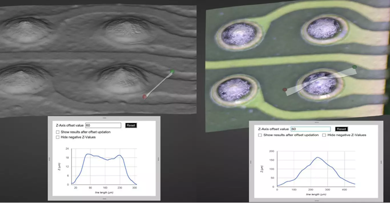
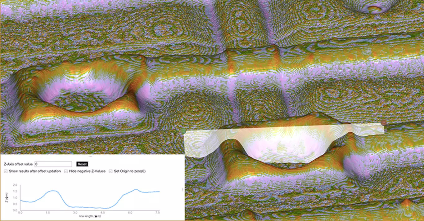
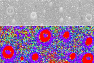
Shown here is an IRQS output of a 200mm bonded silicon wafer pair with embedded metal pads, capturing voids, inclusions, and strain fields. Despite embedded metals, the IRQS System precisely maps defects around these pads.
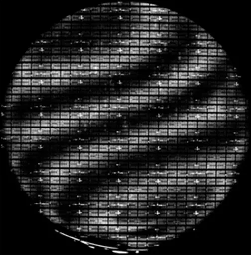
Provides strain field signatures on metallized test wafers, crucial for advanced production monitoring.
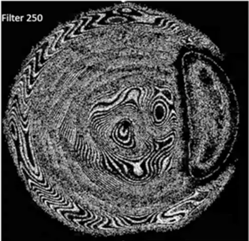
Of course the IRQS System is an ideal production tool for the SiC chip manufacturing environment since it allows detailed analysis of substrate crystal defects and associated strain fields as shown here.
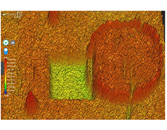
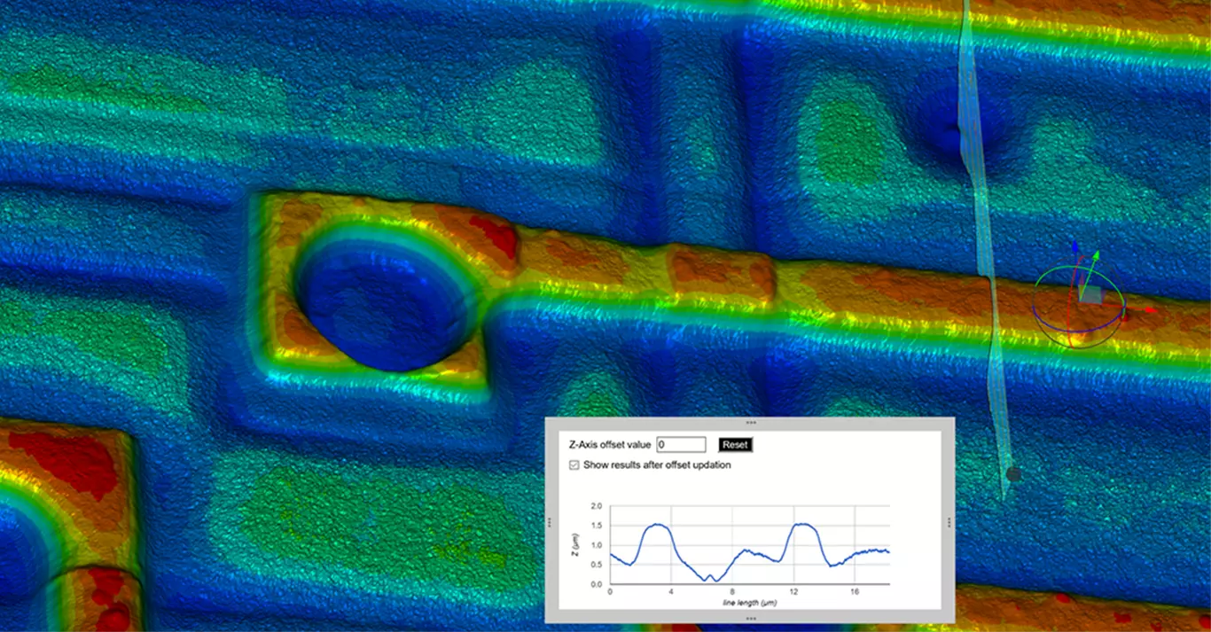
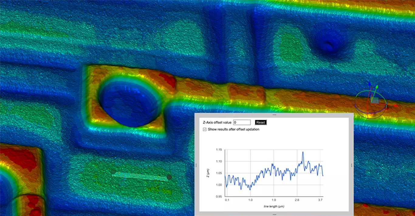
Produces 3D Viewer outputs for in-depth defect visualization.
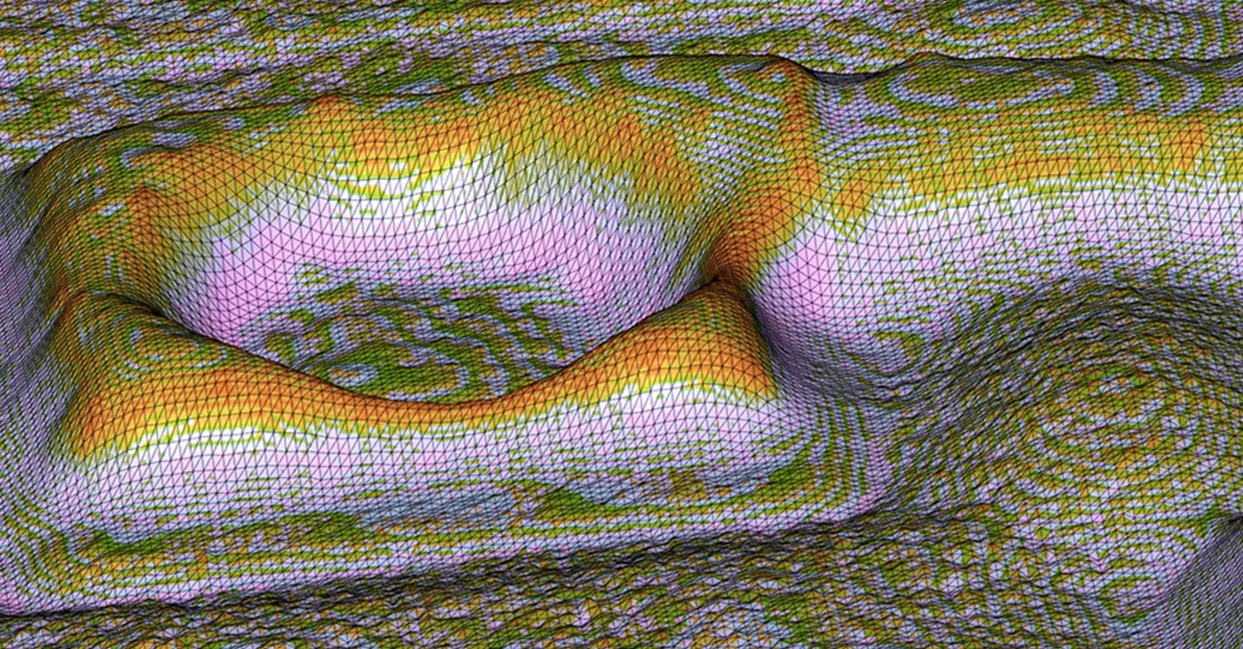
This is an IRQS System 3D Viewer output from the far right side of the same bonded wafer pair showing the details of a metal pad and the large void adjacent to it. It should be noted that although metal pads exist within the bonded pair of silicon wafers the IRQS System is able to provide data in and around these pads.
The core value which drives the design of our systems is EASE OF USE. But we didn't stop there, in fact we started with our proprietary and patented imaging technology and built a full system around it. Then we added our core expertise in Artificial Intelligence.
Introducing BPT Clarity IRQS micro system through substrate inspection
Features
Out performs other systems in the market

Proprietary IRQS System
View voids clearly with IRQS
Multi Platform Software compatible with SEMI Standards
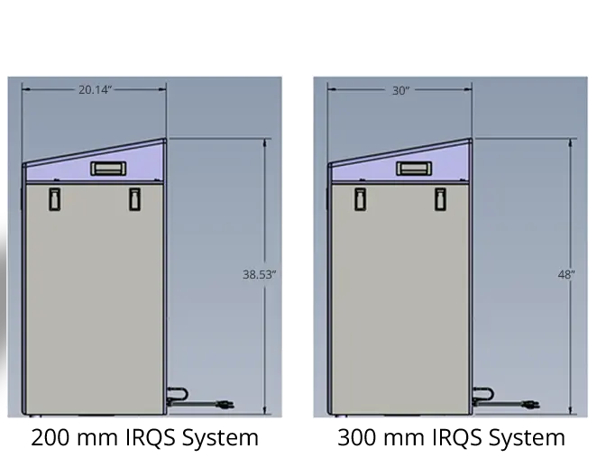
Supports substrates up to 300mm (open platform design)
Automation customized for throughput & sample size
Clarity Pro software for turnkey solution measurements to SEMI standards
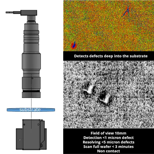
Sub-micron resolution for Voids & Strain Fields
High dynamic range scanning
High pixel resolution for high-detail imaging
Automation ready for high-throughput fab environments
BOLTS configuration for attachment to any EFFEM or process tool
Full wafer scan with 2-3mm edge exclusion
KLARF-like file outputs for precise location review
Turnkey recipe setup software for quick deployment
Lowest cost
Brochure