Detect. Measure. Classify. Learn. Improve.
One connected platform for semiconductor process control
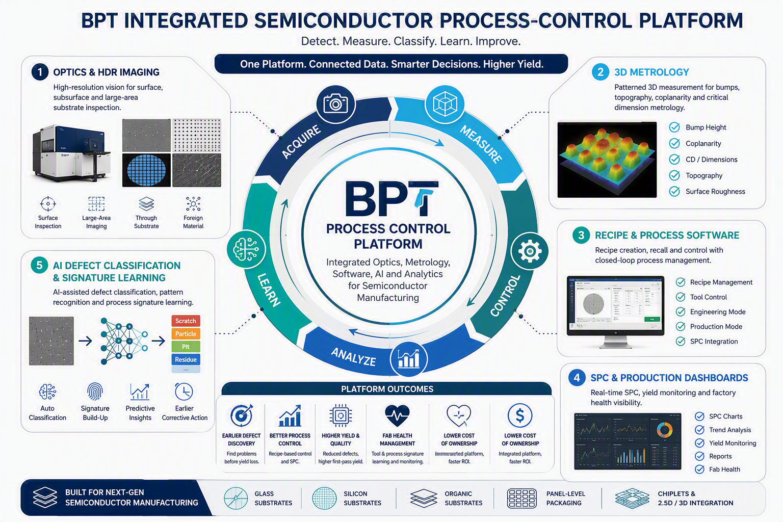
BPT brings advanced optics, patterned 3D metrology, production software, SPC, reporting and AI-enabled defect intelligence into a common manufacturing platform. The architecture supports front-end and back-end workflows across glass, silicon, organic substrates and advanced packaging.
The platform connects:
- High-resolution HDR optical inspection for surface, subsurface and large-area applications
- Patterned 3D measurement for bumps, coplanarity, dimensions, topography and surface roughness
- Recipe management, production control, SPC, reports and dashboards
- AI-assisted defect classification and process-signature learning

Proven in manufacturing. Validated by a top-tier customer.
BPT technology has moved beyond development into a customer-deployed semiconductor manufacturing environment.
Delivered
Engineered and delivered for a demanding semiconductor manufacturing application.
Installed
Deployed within a top-tier customer environment.
Validated
Core inspection, metrology, software and workflow capabilities validated by the customer.
Manufacturing-ready
Execution demonstrated from system design through deployment and support.
BPT is not a laboratory concept. It is a deployed, customer-validated platform built for real semiconductor manufacturing requirements.
Earlier defect discovery. Better process control.
Next-generation materials and packaging structures require inspection data that goes beyond images.
Emerging materials
Inspection optimized for glass, new substrate formats and evolving characteristics.
Advanced packaging
HBM, chiplets, 2.5D/3D integration and bump structures increase measurement complexity.
Yield excursions
Detect defects and tool signatures before manufacturing impact escalates.
Manual review
AI-assisted classification reduces dependency on repetitive defect review.
Unified inspection and metrology platform
Inspection becomes more valuable when optics, metrology, recipes, SPC, reporting and classification data are connected.

High-resolution optical inspection
Flexible optical inspection supports surface, subsurface, large-area and foreign-material applications.
- HDR imaging: preserve defect visibility across reflective and transparent surfaces.
- Large-area inspection: production-oriented scanning and automation for large formats.
- Multiple inspection modes: glass, silicon and advanced substrates.
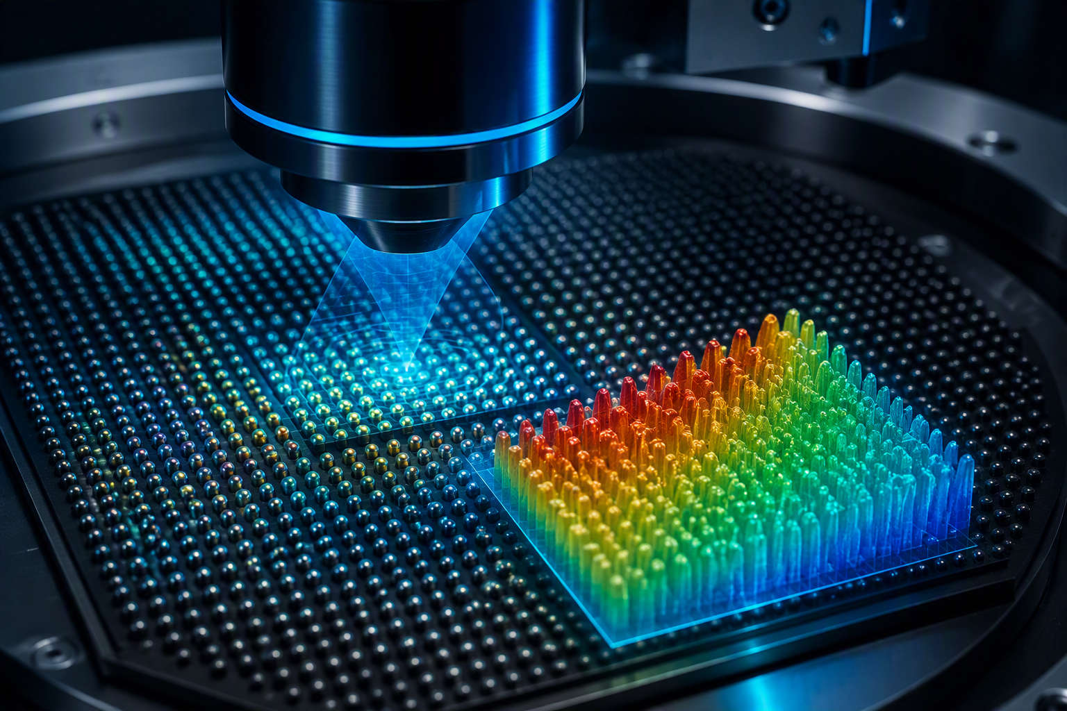
3D metrology for advanced packaging
Patterned 3D measurement supports critical dimensional and surface metrics with production-ready data for process control.
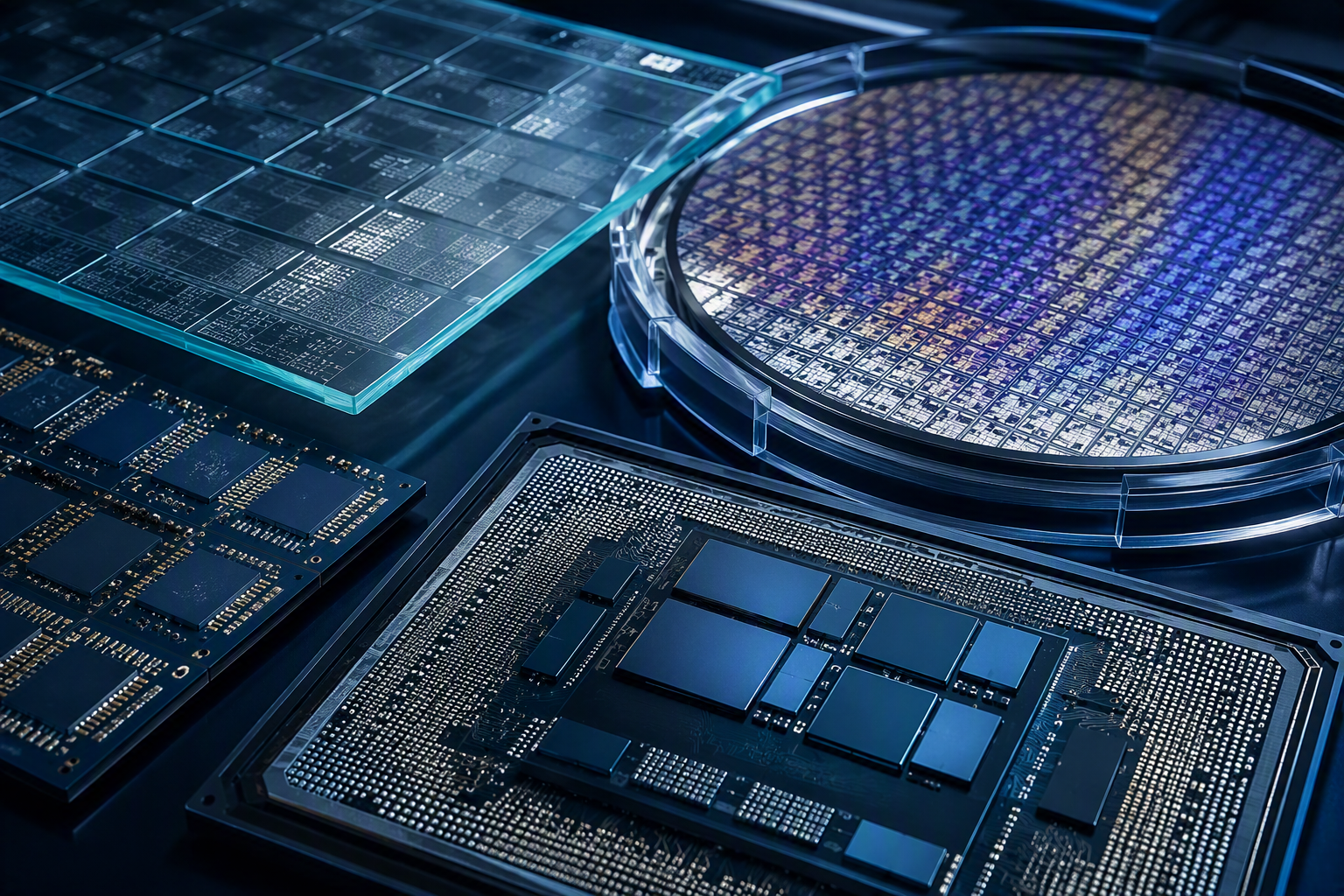
A common architecture across substrate types
The same inspection, metrology and AI foundation can be configured for multiple manufacturing needs.
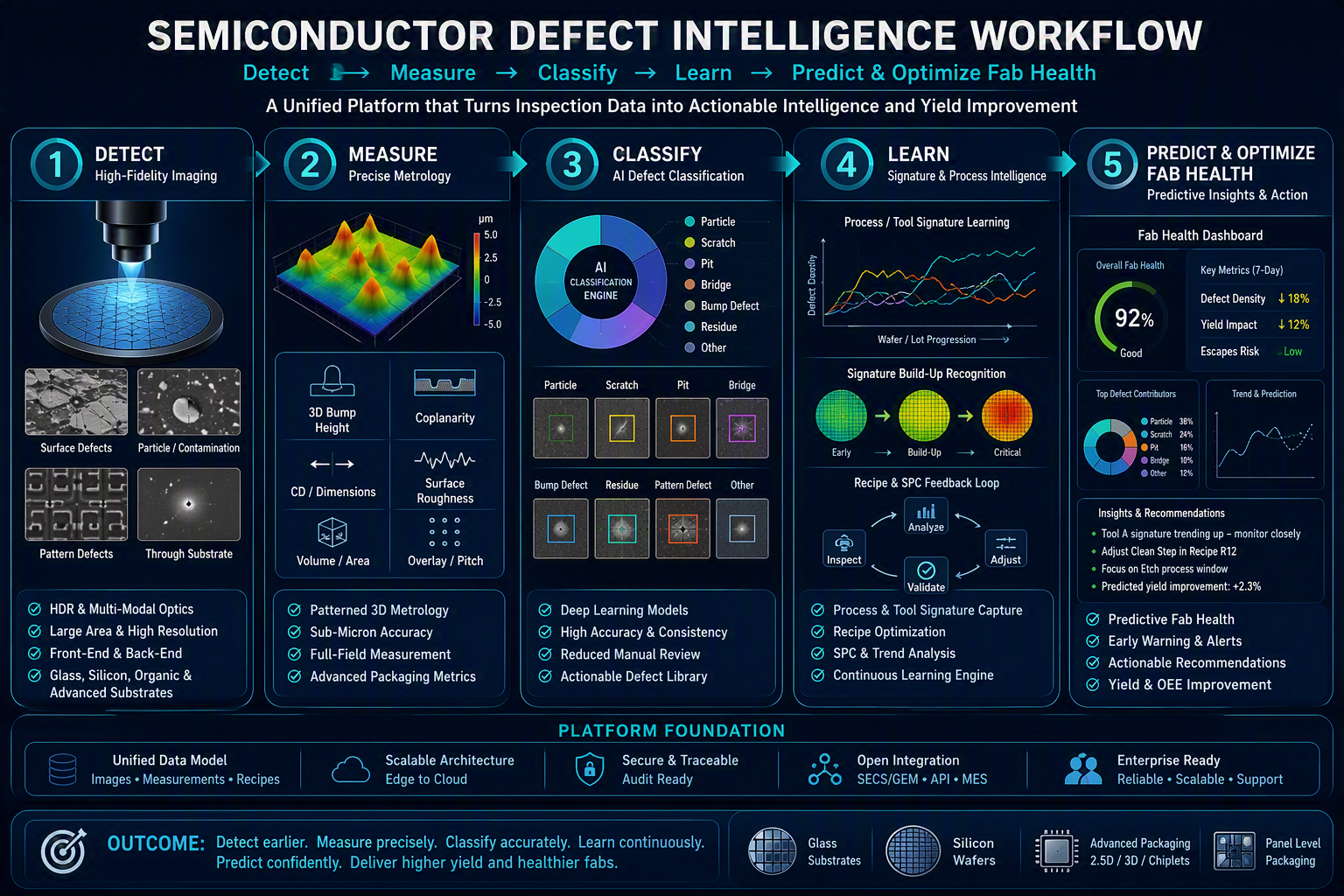
AI defect intelligence
Connected defect and measurement data supports signature learning and earlier process insight.
From engineering setup to production control
Recipe management, SPC, reporting and dashboards connect inspection to manufacturing workflows.
Create
Define recipes
Recall
Deploy controlled recipes
Inspect
Capture production data
Analyze
Review SPC and trends
Improve
Feed insight to control
Control
Improve process health

A practical path from inspection data to manufacturing action
Earlier discovery
Find developing signatures before larger yield impact.
Better measurement
Combine inspection with critical 3D and dimensional data.
Faster classification
Organize defect classes and reduce repetitive review.
Smarter process control
Connect recipes, SPC, reports and signature learning.
Bring your next inspection and metrology challenge to BPT.
Substrate inspection • 3D metrology • AI defect classification • process analytics • strategic collaboration
CONTACT BPTGlass Defect Inspection with sub-micron capability
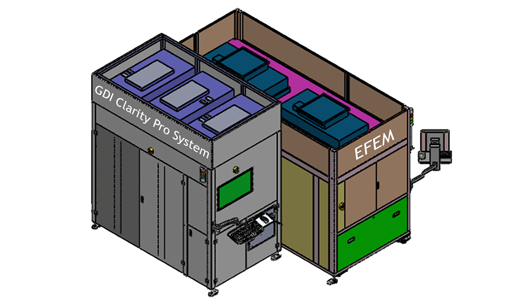
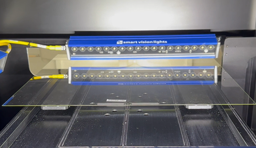
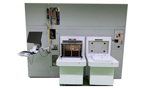
GDI Clarity Pro redefines precision in glass defect inspection with cutting-edge optics and advanced surface scanning. Capable of detecting defects as small as sub-micron levels with a spatial resolution of 2.5 µm, it delivers unmatched edge and through-surface defect analysis. Defect classification & measurement done real-time, with no throughput overhead.
The system offers:
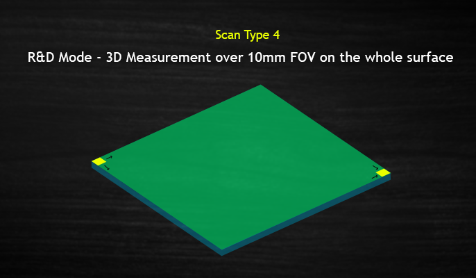
- Production Mode: 35 Panels per Hour, Edge inspection Top & Through Surface 10mm using 3 Probes
- Advanced R&D mode with 2D and 3D inspection capabilities with Z-axis resolution of <1 nanometer
- Full-panel macro-surface scanning for holistic defect identification
- 30mm edge-detection range for surface inspection
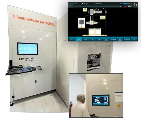
Engineered for Semiconductor industries demanding the highest quality. GDI Clarity Pro brings absolute transparency to defect detection.
How it works
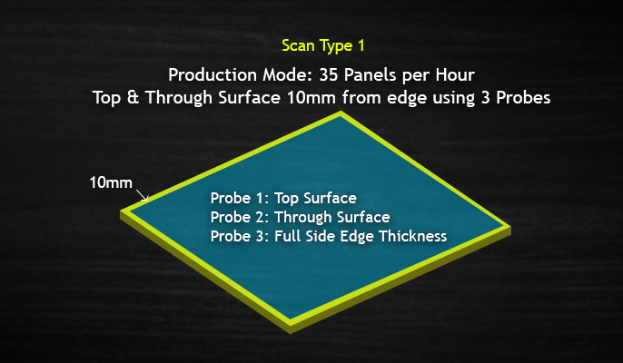
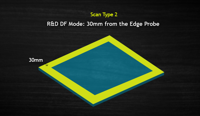
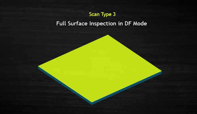
Highlights
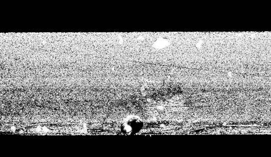
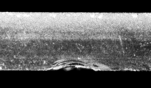
DEFECTS ON GLASS SUBSTRATES
Chips <1 μm
Edge defects <1 μm
Cracks <1 μm length and ≥5 μm depth (in Z)
Scratches <1 μm length and <5 μm depth (in Z)
FM (foreign material) <1 μm
Surface Pitting <1 μm
Stains and FM are classified separate from other defect types
Classification >5 μm
E-MCBFp* > 20,000 cycles with uptime >95%
Supplier dependent scheduled downtime <1%
Substrate Form Factor Size(s) Less than 520mm
Production Run Rate 35 full substrates/hour
Automatic Defect Classification (ADC) Yes
Image Processing Fully Trained AI
Defect Size Repeatability 3-sigma < 10%
Same defect measured at least 20 times to calculate 3-sigma.
Defect Image Capture
Variable magnification review image automatically
saved for visual defect review/classification
R&D Applications
3D-Profile(Mapping) with Z-Height Measurement (>1nm)
Active Area Surface 10mm Inspection Sampling
Equipment Matching/Calibration
Calibration done using Polystyrene or Glass Spheres
Maximum substrate warpage 5mm
Substrate thickness range :
200 microns to 10mm thickness
Automated loading 520mm substrates.
Manual loading <520mm substrates.
Cleanroom Requirement
Class 100
Equipment internal
Class 10
Electrostatic Discharge (ESD)
Ionizer performance±3V
FACILITIES & ELECTRICAL SPECIFICATIONS
Voltage 208 V AC
Number of Phases 1 Phase
Wiring Configuration 3 Wire, 1 Line, 1 Neutral, 1 Ground
Frequency 50/60 Hz
Full Load Current 36 Amps
Non-Continuous Current 12 Amps
Continuous Current 24 Amps
Machine OCP Device Rating 50 A
Ampere of Largest Load 20 A
Air 100 Psi
Vacuum -85 Kpa
SemiConductor Fab Host Fully SEMI Compatible
Application Features

Follows SEMI Standards for Job Handling

Recipe Management

User and Role Management
Access Control Based on Login

Defect/Particle Map in Standard Format

Charting Package for Professional Reporting

3D Viewer with Measurements
Die-to-Die Matching

2D and 3D Analysis

HDR Imaging

Edge Inspection

A.I. Available for Classifying Defects & Tagging defects

Signature Analysis